Automated Test data collection for Yield Improvement using Wafer Mapping Analysis
The Semiconductor industry has a complex multi-stage manufacturing process, with great focus on high yield and quality improvement as a continuous effort to meet the ever-growing demand in the industry. One of the key requirements for a complete defect traceability analysis, is to have the infrastructure set up to collect test measurement data to provide the analysis required to proactively prevent costly quality incidents. This test data is often called as Wafer test data or Device test data, and is the key source of information in generating what is called as a “Wafer Map”, which in-turn provides a graphical representation of Wafer test results for a given test program step.
Two types of Test Measurements
There are primarily two types of semiconductor test data – At the end of the fabrication process, the fab electronically tests each individual chip on a wafer. This is called unit probe or wafer test. Based on the test results, each chip on the wafer gets grouped to a certain bin category mostly named as bin 1, bin 2, etc. Generally, bin 1 is a “pass” and bin 2 through the rest is a “fail” and each number represents a category/cause of the failure. The chips are again tested after the packaging to make sure that all packaging components are in place as needed, as well as it is meeting the desired Analog performance. This is referred to as “final test”. This data plays a key role during wafer assembly and packaging in addition to being the key input for wafer mapping analysis.
Wafer Mapping Methods
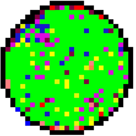
Many studies show that yield improvement can be easily found in probe tests. Hence, making the wafer test measurement data easily accessible in the proper shape, is critical in enabling wafer mapping. Below image shows a typical wafer map.

As shown in the image, different bins are represented by different colours. This wafer map is generated from extensive amounts of production data, which is the spatial measurements on die coordinates in a wafer. Advanced manufacturing test facilities today, can collect and store this data typically in enterprise data warehouse and other Big Data platforms, making it feasible to do this cutting edge spatial/zonal analysis. Now, making the data available in traditional methods only helps to generate simple summaries like overall yield. Unless this data is transformed in to meaningful wafer map images, we are missing the opportunities for process improvement that can be revealed using various structural patterns in the map.
Topology Specification – A key component for wafer mapping
Given that wafers can be tested in different orientations in different equipments and programs, the topology specification becomes key in creating the wafer maps. Topology specification in this context is a set of attributes that defines the orientation information for a given product family wafer. The key elements include – Notch angle, X/Y direction/orientation. As the initial set up is done in the Electronic wafer mapping system, a wafer notch is derived on the wafer. Usually, this is a physical mark and is the lower edge of the wafer in a relational co-ordinate system, with X axis increasing towards right and Y axis increasing upwards. This wafer notch helps to identify the relative position of the wafer with respect to uniform co-ordinate system. The topology specification is usually derived from systems like EWM (Electronic wafer mapping), and stays constant for a given product family.
Using this topology specification information, test measurement data from different test programs, are transformed into a uniform co-ordinate system. This will allow various wafer mapping tool to create a graphical representation of the wafer map showing various bin values with colour coding, thereby providing grater insight to spatial structures identifying various defect patterns resulting in new opportunities for process and yield improvements. The wafer maps later get divided in to various spatial zones, and zonal yield calculations are done there by detecting and fixing various process issues resulting in yield and quality improvement.
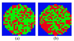
A typical example of process yield improvement using wafer mapping analysis is the defect cluster recognition. Usually, any defects caused by a systematic problem during wafer fabrication process forms a unique pattern on the wafer map. These are referred to as defect clusters and is represented as a group of dies/parts failing together in wafer map. Below image has two wafer maps. Figure (a) shows random die failures, whereas figure (b) shows a defect clusters. Different defect patterns are identified from this analysis, and are tied back to a certain systematic failure caused during the wafer manufacturing process. This process plays key role in manufacturing yield improvement, and studies shows that real-time process control using defect cluster recognition helps to achieve 95% accuracy required by several product types.

Benefits of Automated data collection for Wafer Mapping
Given the focus on quality and cost, it becomes inevitable for a semiconductor manufacturing operation, to have an automated data collection and storage of test measurement data for wafer mapping, to enable yield loss calculations and operational efficiency. This indirectly helps the engineers to spend more time on critical operational issues than worrying about collecting data and shaping it for the zonal analysis. As test programs are adopting more in-built intelligence and automated frameworks, the volume of test data is also becoming significantly huge. Also, test data from different sub-contracting test facilities needs to be integrated together to do modern analytics of merging wafers in a map for dissection analysis of various hard and soft bins. So, it becomes significantly important to have a centralized robust test measurement data collection and transformation system to enable wafer mapping capabilities, thereby improving yield, cycle time and overall process efficiency.
Latest Blogs
Core banking platforms like Temenos Transact, FIS® Systematics, Fiserv DNA, Thought Machine,…
We are at a turning point for healthcare. The complexity of healthcare systems, strict regulations,…
Clinical trials evaluate the efficacy and safety of a new drug before it comes into the market.…
Introduction In the upstream oil and gas industry, drilling each well is a high-cost, high-risk…


